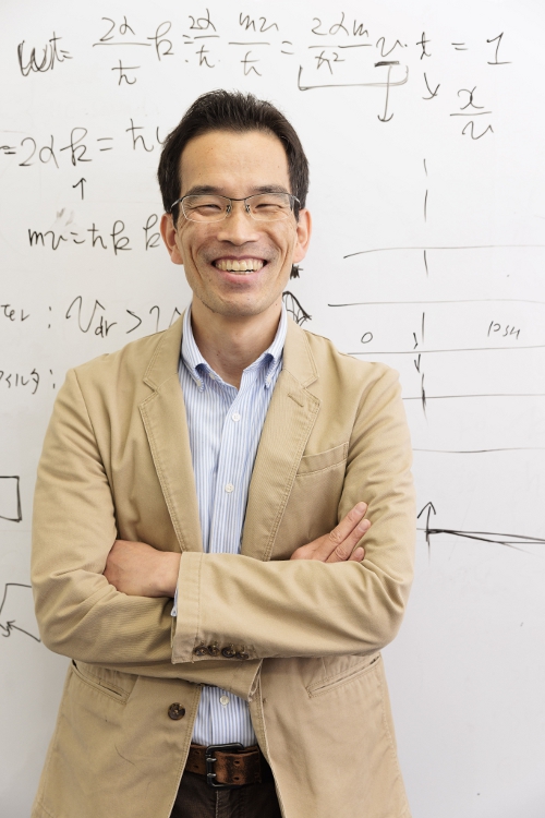
Profile.

Kohda Laboratory.

Makoto Kohda


東北大学大学院工学研究科 知能デバイス材料学専攻
情報デバイス材料学講座 電光子情報材料学分野
好田研究室

works
contact

Profile.

Kohda Laboratory.

Makoto Kohda


東北大学大学院工学研究科 知能デバイス材料学専攻
情報デバイス材料学講座 電光子情報材料学分野
好田研究室

my works
contact

好田 誠

Kohda Makoto

大学院工学研究科・工学部 知能デバイス材料学専攻
教授、工学博士
専門分野 スピントロニクス


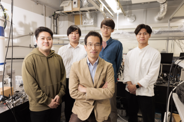
Research activities and collaboration network
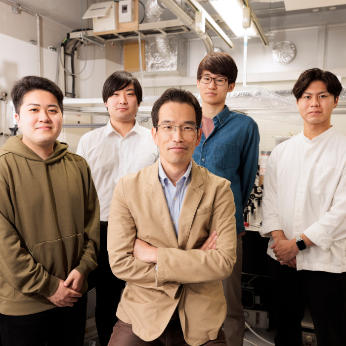
好田誠教授の画像
好田誠教授と学生の画像

研究は驚きと感動の連続


研究を行っていると、これまで誰も見たことの無い物理現象や法則、そして新しい考え方に日々遭遇します。
そして驚きや感動を味わうことができます。
その理由は、これまでのみなさんが行ってきた勉強では「答え」が予め用意されていましたが、 研究では「答え」を自ら用意する=解き明かすその過程が楽しいからだと思います。
研究室では、世界の一線で活躍しているみなさんの先輩たちが待っています。
是非、私たちと共に未来を創っていきましょう。

好田誠教授と学生の画像

My works

What’s new

2022年3月

半導体細線構造では電子の運動方向が一方向に決まるため有効磁場の向きが一軸となりますが、その有効磁場と外部磁場がどのような競合を見せスピン緩和が決まるのかに関して理論・実験共に理解されてきませんでした。 半導体細線構造における有効磁場と面内外部磁場下でのスピンダイナミクスの理論を構築し、予言されていたスピン緩和時間と歳差運動周波数の異方性を時間分解カー回転測定より実験的に明らかにすることに成功しました。
“Anisotropic spin dynamics in semiconductor narrow wires from the interplay between spin-orbit interaction and planar magnetic field”, Junpei Sonehara, Michael Kammermeier, Dai Sato, Daisuke Iizasa, Ulrich Zülicke, Shutaro Karube, Junsaku Nitta, and Makoto Kohda, Physical Review B,105, 094434 (2022).

2022年3月

InGaAsなどの狭ギャップ半導体ではDPスピン緩和機構と共にEYスピン緩和機構が共存する系になりますが、互いのスピン緩和時間を定量的に見積もることはスピン緩和の起源が異なるために困難でした。
DPスピン緩和は電子速度に依存すること(スピン拡散)を利用して、DPスピン緩和時間とEYスピン緩和時間を分離し定量的に求めることに成功しました。千葉大森田教授との共同研究です。
“Dyakonov–Perel and Elliot–Yafet spin relaxation rates in InGaAs/InAlAs multiple quantum wells at room temperature”, Ayuki Yasuhito, Koichi Shota, Kyohei Nobuhide, Makoto Kohda, and Ken Morita, Applied Physics Express 15, 043001 (2022).

過去のWhat’s new(クリックで読む)

2021年12月

弱反局在理論は半導体中のスピン緩和時間を定量的に求める方法としてよく知られていますが、取り扱うモデルにより近似の仕方が異なるため、それがスピン軌道相互作用の物性値を正確に求める上で差を生み出していました。
代表的な2種類の弱反局在理論に対し互いの矛盾を明らかにし、永久スピン旋回状態近傍で高精度にスピン緩和時間を求める理論的枠組みを構築しました。
“Reliable modeling of weak antilocalization for accurate spin-lifetime extraction”, Michael Kammermeier, Takahito Saito, Daisuke Iizasa, Ulrich Zülicke, and Makoto Kohda, Physical Review B,104,(2021), 235430.

2021年10月

10月21日木曜日TBCラジオ(エンボヤージュ)のパーソナリティーズノーズ(9:15-)に出演しました。
最先端の研究を分かりやすくお伝えする企画を熊谷望那アナウンサーが立ち上げて下さり、現在行っている研究をお話ししました。
“未来のスマホも二刀流?!電子のスピンで叶える2050年コンピューターの世界”.

2021年8月

遷移金属カルコゲナイドは大きなスピン分裂とバレー自由度を持つためスピンの緩和過程が複雑となります。その中でもバレー内緩和はスピンの向きだけでなくAエキシトンからBエキシトンへと遷移する緩和機構でもあるので重要ですが、バレー偏極率に及ぼす影響は分かっていませんでした。
単層MoS2において、Bエキシトンを励起するとバレー内緩和を経てAエキシトンとして発光するパスがあることを定常状態のバレー偏極率から同定することに初めて成功しました。
“Intravalley Scattering Probed by Excitation Energy Dependence of Valley Polarization in Monolayer MoS2“, Eito Asakura, Takeshi Odagawa, Masaki Suzuki, Shutaro Karube, Junsaku Nitta and Makoto Kohda, Journal of Physics D: Applied Physics, 54, 485304 (2021).

2021年7月

時間分解カー回転法では、通常半導体量子構造を有する薄膜面内の有効磁場をスピン拡散から求められますが、薄膜垂直方向に存在する有効磁場は、光励起の電子スピンと有効磁場が平行となるため歳差運動せず検出が困難でした。
有効磁場が薄膜面内と面直双方に存在する(110)面InGaAs量子井戸を用いて、面内/面直有効磁場を室温で定量評価できる新たな方法を確立しました。千葉大森田研・産総研・筑波大との共同研究です。
“Room-temperature spin–orbit magnetic fields in slightly misoriented (110) InGaAs/InAlAs multiple quantum wells”, Koichi Nakanishi, Ayuki Arikawa, Yasuhito Saito, Daisuke Iizasa, Satoshi Iba, Yuzo Ohno, Nobuhide Yokota, Makoto Kohda, Yoshihiro Ishitani, and Ken Morita, Applied Physics Letters,119,(2021), 032405.

2021年3月

応用物理学会から2021年APEX/JJAP編集貢献賞を頂きました。
関係者の皆様に感謝いたします、有難うございました。

2021年3月

半導体1次元構造はマヨラナ準粒子などトポロジカル量子計算を可能にする舞台です。その時、スピン軌道相互作用は極めて重要な物理量になりますが、1次元構造では弱局在現象が支配的となるため、弱反局在を用いたスピン軌道相互作用の定量評価法が通用しない、基本的な課題が残されていました。
面内磁場を印加することで誘起される弱局在の異方性から、III-V族半導体1次元構造に存在する全てのスピン軌道相互作用を定量評価できる初めての方法を確立しました。
“Full spin–orbit coefficient in III–V semiconductor wires based on weak localization anisotropy under in-plane magnetic field”, Toshimichi Nishimura, Kohei Yoshizumi, Takahito Saito, Daisuke Iizasa, Junsaku Nitta and Makoto Kohda, Physical Review B,103,(2021), 094412.

2021年1月

スピン緩和時間が結晶方向に依存するとスピン緩和に異方性が生まれます。この異方性はスピン軌道相互作用に由来するので物質固有値であると考えられてきましたが、実は制御できることを初めて示しました。
III-V族半導体で明らかになった今回のスピン緩和異方性の制御は、トポロジカル物質や酸化物、原子層物質にもあらわれる可能性があります。
“Control of Spin Relaxation Anisotropy by Spin-Orbit-Coupled Diffusive Spin Motion”, Daisuke Iizasa, Asuka Aoki, Takahito Saito, Junsaku Nitta, Gian Salis, Makoto Kohda, Physical Review B,103,(2021), 024427.

2020年12月

第14回青葉工学振興会賞を受賞しました。
半導体における新規スピン制御原理の確立と長距離スピン輸送に関する研究に対して頂きました。
どうも有難うございました。

2020年6月

III-V族半導体においてスピン緩和を抑制できる有力な手法として「永久スピン旋回状態」がありますが、この状態が最も安定となる結晶方位を理論的に明らかにしました。
これまで全く研究がされてこなかった225面が最も安定であることを示しました。本論文はPRBのEditor’s Suggestionに選ばれました。
“Enhanced longevity of the spin helix in low-symmetry quantum wells”, Daisuke Iizasa, Makoto Kohda, Ulrich Zülicke, Junsaku Nitta, Michael Kammermeier, Physical Review B,101,(2020), 245417.
プレスリリース(東北大学).
プレスリリース(工学研究科).
プレスリリース(マテリアル系).
プレスリリース(FRiD).
電波新聞.
プレスリリース英語版(Press Release in English).
EurekAlert.
日刊工業新聞.

2020年3月

スピン軌道ロッキングを用いたスピン制御に関する論文が、2019年のScientific Reportsにおいて物理学Top100ダウンロード数論文として選ばれました。
様々な物質界面に存在するスピン軌道ロッキングがスピン制御に初めて利用できた内容です。ご興味のある方はご覧ください。
Top 100 in Physics 2019
Scientific Reports,9,(2019),1909.

2020年3月

日本金属学会 功績賞を受賞しました
スピン軌道相互作用を利用したスピン・磁化の電気的制御に関する研究に対して頂きました。どうも有難うございました。

2019年10月

スピン波が形成される前のトランジエントな領域においてもスピン拡散からスピン軌道相互作用を求められることを示しました。
千葉大学森田准教授との共同研究です。スピン波が励起できるミクロ領域でも平面波励起のマクロ領域でもユニバーサルにスピン拡散現象が働いていることを明らかにしました。
“Transient diffusive spin dynamics in intrinsic InGaAs/InAlAs multiple quantum wells” K. Kawaguchi, T. Fukasawa, I. Takazawa, H. Shida, Y. Saito, D. Iizasa, T. Saito, T. Kitada, Y. Ishitani, M. Kohda, and K. Morita
Applied Physics Letters,115,(2019),172406.

2019年7月

拡散とドリフト運動がスピン歳差運動に与える影響を調べました。スピン軌道相互作用が生み出す有効磁場を高精度に評価できます。
GaAs量子井戸において拡散運動とドリフト運動が支配するスピン歳差運動の様子を分離して捉えることに成功しました。どちらの運動も有効磁場を生み出すのですが、その違いを明らかにすることができました
“Simultaneous evaluation of drift- and diffusion-induced spin-orbit fields in a (001) GaAs/AlGaAs two-dimensional electron gas” T. Saito, A. Aoki, J. Nitta, and M. Kohda
Applied Physics Letters,115,(2019),052402.

2019年5月

単層MoS2におけるバレー偏極とバレーコヒーレンスの同時制御を実現しました。バレー量子情報の基盤技術となります。
遷移金属カルコゲナイドMoS2におけるKとK’バレーの偏極とコヒーレンス生成を光学的に検出しました。バレー自由度を自在に制御する上で、バレー偏極とバレーコヒーレンスはスピン偏極とスピンコヒーレンスに対応した重要な要素技術ですが、光学的に自在に生成できることを示しました。光学的なバレー量子情報の重要なステップとなります。
“Detection of both optical polarization and coherence transfers to excitonic valley states in CVD-grown monolayer MoS2” E. Asakura, M. Suzuki, S. Karube, J. Nitta, K. Nagashio and M. Kohda
Applied Physics Express,12,(2019),063005.

2019年2月

半導体における高効率スピン制御法を実現しました。スピン軌道ロッキングと呼ばれる手法を用いた新たなスピン回転制御の確立となります。
スピン緩和を抑制しながら効率的にスピン制御を可能にする新たな原理を実証しました。スピン軌道ロッキングを用いることで、常に電子スピンが有効磁場方向に揃いながらスピン制御できるためスピン緩和が抑制され、量子情報やスピントロニクスなどに大きく貢献することが期待されます。
“Spin-momentum locked spin manipulation in a two-dimensional Rashba system”
M. Kohda, T. Okayasu and J. Nitta
Scientific Reports,9,(2019),1909.

2018年12月

RIEC Award 東北大学研究者賞を受賞しました
半導体量子構造における電気的スピン生成とスピン緩和抑制に関する研究に対して頂きました。どうも有難うございました。

2018年10月

(001)と(110)量子井戸で実現できる永久スピン旋回状態の本質的な違いを明らかにしました
面方位が異なりますが(001)と(110)量子井戸ではどちらも永久スピン旋回状態を実現できます。しかし、ドレッセルハウススピン軌道相互作用の高次項の対称性がことなるため、永久スピン旋回状態の寿命は大きく異なることを理論的に見出しました。
“Robustness of a persistent spin helix against a cubic Dresselhaus field in (001) and (110) oriented two-dimensional electron gases”
D Iizasa, D. Sato, K. Morita, J. Nitta, and M. Kohda,
Physical Review B,98,(2018),165112.

2018年7月

第17回インテリジェントコスモス奨励賞を受賞しました
半導体量子構造における電気的スピン生成と長距離スピン輸送に関する研究に対して頂きました。どうも有難うございました。

2018年4月

文部科学省 若手科学者賞を受賞しました
スピン軌道相互作用を用いたスピン生成とスピン輸送に関する研究に対して頂きました。どうも有難うございました。

2018年1月

層状物質GaSeにおけるスピン軌道相互作用および導波路効果に関する論文を発表しました
GaSeのスピン軌道相互作用の評価と層状物質特有の導波路効果について研究を2本論文にまとめました。GaSeはスピントロニクスにおいても光学素子としても、とても面白い物性を有しています。
“Weak antilocalization induced by Rashba spin-orbit interaction in layered III-VI compound semiconductor GaSe thin films”
S. Takasuna, J. Shiogai, S. Matsuzaka, M. Kohda, Y. Oyama,and J. Nitta
Physical Review B Rapid Communications,96,(2017),161303(R).
“Effect of optical waveguide on photoluminescence polarization in layered material GaSe with millimeter scale”
M. Suzuki, M. Kohda, S. Takasuna, S. Matsuzaka, Y. Sato, T. Tanabe, Y. Oyama,and J. Nitta
Japanese Journal of Applied Physics,57,(2018),020308.

2017年7月

永久スピン旋回状態に関するレビュー論文を発表しました
半導体におけるスピン軌道相互作用と永久スピン旋回状態についてこれまでの研究をまとめました。
初学者にもできるだけわかるように式の導出と物理的な意味を書きましたのでご参考にして頂ければと思います。
“Physics and application of persistent spin helix state in semiconductor heterostructures”
M. Kohda and G. Salis
Semiconductor Science and Technology,32,(2017),073002. (doi.org/10.1088/1361-6641/aa5dd6)

2016年8月

エピタキシャルPt薄膜のスピン緩和機構を解明しました
エピタキシャルPt薄膜におけるスピン緩和は半導体と同じくDyakonov-Perel機構であることを初めて明らかにしました。
金属極薄膜でも電気的なスピン制御が可能であることを意味しています。
“Observation of the D’yakonov-Perel’ spin relaxation in single-crystalline Pt thin films”
J-C. Ryu, M. Kohda, and J. Nitta
Physical Review Letters,116,(2016), 256802-1-256802-6. (doi:10.1103/PhysRevLett.116.256802)

2016年7月

永久スピン旋回状態におけるドリフトスピン輸送を実現しました
永久スピン旋回状態ではスピン緩和が抑制されるため100ミクロン以上までスピンを電界で輸送することが可能です。内部対称性に守られた永久スピン旋回状態の面白さがデバイス応用に利用できる可能性があります。
“Drift transport of helical spin coherence with tailored spin-orbit interactions”
Y. Kunihashi, H. Sanada, H. Gotoh, K. Onomitsu, M. Kohda, J. Nitta, and T. Sogawa
Nature Communications,7,(2016),10722. (doi:10.1038/ncomms10722)

2016年6月

InGaAs量子井戸を用いて永久スピン旋回状態とその逆状態の電気的制御を実現しました
永久スピン旋回状態はスピン制御と長距離スピン輸送を同時に実現できる面白い状態です。永久スピン旋回状態とその逆状態のゲート制御によりスピンロジック回路の実現が期待できます。
“Gate-controlled switching between persistent and inverse persistent spin helix states”
K. Yoshizumi, A. Sasaki, M. Kohda, and J. Nitta
Applied Physics Letters,108,(2016),132402-1-132402-4. (doi:10.1063/1.4944931)

2016年5月

電子のドリフト運動と拡散運動におけるスピン歳差運動の差から
バルクDresselhausスピン軌道相互作用係数を高精度に求める手法を確立しました。
電子スピンはドリフト運動と拡散運動では異なる有効磁場を感じています。
これをうまく利用することでバルクDresselhausスピン軌道相互作用係数を求めることが可能となります。
“Current-Controlled Spin Precession of Quasistationary Electrons in a Cubic Spin-Orbit Field”
P Altmann, F. G. G. Hernandez, G. J. Ferreira, M. Kohda, C. Reichl, W. Wegscheider, and G. Salis
Physical Review Letters 116, 196802-1-196802-4 (2016). (doi: 10.1103/PhysRevLett.116.196802)

2015年12月

準1次元的な閉じ込め効果を用いることでヘリカルスピン構造を半導体中で実現しました。
細線構造における時間空間分解Kerr測定から横方向の閉じ込め効果が強くなるに従い、ヘリカルスピン構造が現れスピン緩和時間が増大することを示しました。
“Transition of a two-dimensional spin mode to a helical state by lateral confinement”
P.Altmann, M. Kohda, C. Reichl, W. Wegscheider, and G. Salis.
Physical Review B92, 235304-1-235304-6 (2015). (DOI:10.1103/PhysRevB.92.235304)

2015年10月

電子の拡散運動を利用して2種類のスピン軌道相互作用を別々に評価する手法を確立しました。
時間・空間分解Kerr測定法を用いて電子の拡散に伴い生じる有効磁場を高感度に光検出し、RashbaおよびDresselhausスピン軌道相互作用の係数を求めることに成功しました。IBMチューリッヒ研究所で行った研究をまとめたものです。
“All-optical evaluation of spin-orbit interaction based on diffusive spin motion in a two-dimensional electron gas”
M. Kohda, P Altmann, D. Schuh, S. D. Ganichev, W. Wegscheider, and G. Salis
Applied Physics Letters 107, 172402 (2015). (doi: 10.1063/1.4934671)

2014年~2015年3月

IBMチューリッヒ研究所にて時間分解スピン計測法を学んできました。
時間分解Kerr測定法による光学測定を用いたスピン軌道相互作用に関する研究を行ってきました。今後は磁気伝導測定そして光学測定を合わせてスピン軌道相互作用研究を展開できればと思います。

2014年7月

半導体細線構造を用いて2種類のスピン軌道相互作用の大きさを電気的に検出することを可能にしました。
細線に面内磁場を印加し面内磁場と有効磁場の方向が一致する時とそうでないときでスピン緩和時間に異方性があらわれます。それを磁気伝導として検出することで有効磁場方向を検出できます。
A. Sasaki, S. Nonaka, Y. Kunihashi, M. Kohda, T. Bauernfeind, T. Dollinger, K. Richter, and J. Nitta.
“Direct determination of spin-orbit interaction coefficients and realization of the persistent spin helix symmetry”,
Nature Nanotechnology 13, 703-709 (2014).DOI: 10.1038/NNANO.2014.128

2014年3月

財団法人本多記念会より本多記念研究奨励賞を受賞しました。
受賞理由は、半導体におけるスピン軌道相互作用を用いた電気的スピン生成・制御に関する研究によるものです。

2014年3月

日本応用物理学会誌Vol.83「これからのスピントロニクス」に記事が掲載されました。
半導体において全く磁場を必要としないスピンフィルタと電子スピン共鳴に関する解説記事です。NTT物性基礎研究所眞田治樹主任研究員との共著となります。

2013年10月

日本磁気学会誌まぐねVol.8特集「狭ギャップ半導体およびシリコンスピントロニクスの最近の話題」に記事が掲載されました。
半導体における永久スピン旋回状態のゲート制御に関する解説記事です。
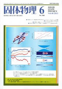
2013年6月

固体物理6月号にスピン軌道相互作用を用いたスピン生成の記事が掲載されました。
シュテルン-ゲルラッハの実験を固体中で実現した研究について分かりやすく解説しています。掲載した図の一部は表紙にもなりました。京大・東邦大・NTTとの共同研究によるものです。

2013年4月

半導体で広く用いられているGaAsとInP基板上に垂直磁化FePdのエピタキシャル成長に成功しました。
InPとGaAs基板上ではL10-FePd/MgOの受ける歪みが異なるので磁気特性が大きく変化します。東北大応用物理学専攻安藤研究室との共同研究で得られた成果です。
“Structural and magentic properties of L10-FePd/MgO films on GaAs and InP lattice mismatched substrates”
M. Kohda, S. Iimori, R. Ohsugi, H. Naganuma, T. Miyazaki, Y. Ando and J. Nitta
Appl. Phys. Lett. 102, 102411(2013)

2013年1月

量子ポイントコンタクトを用いてスピン偏極電流を生成する発表がYoutubeにアップされました。
2013年1月24日慶応大学 Topical workshop on semiconductor spintronicsでの講演です。
ご覧になりたい方はコチラから

2012年8月

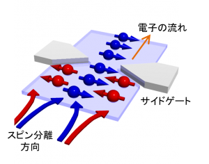
強磁性体や外部磁場を用いずに電子のスピンを揃えることに世界で初めて成功しました。
半導体中でシュテルン-ゲルラッハのスピン分離実験を実現したことになります。
“Spin-orbit induced electronic spin separation in semiconductor nanostructures”
Makoto Kohda, Shuji Nakamura, Yoshitaka Nishihara, Kensuke Kobayashi, Teruo Ono, Jun-ichiro Ohe,
Yasuhiro Tokura, Taiki Mineno, and Junsaku Nitta.
Nature Communications 3, 1082 (2012). (doi:10.1038/ncomms2080)
プレスリリースはこちらから
スピン軌道相互作用に起因する有効磁場の空間勾配を用いて、上向きスピンと下向スピンを空間的に分離し、片方のスピンだけを取り出すことに成功しました(下の図のようなイメージです)。

2012年8月

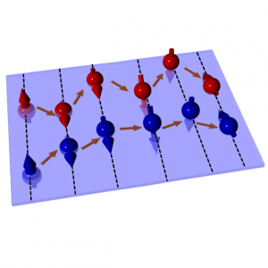
電子スピン永久旋回状態のゲート電界制御に成功しました。
有効磁場が一軸異方性となるため、電子スピン緩和を完全に抑制することが可能となります。
“Gate-controlled persistent spin helix state in (In,Ga)As quantum wells”
M. Kohda, V. Lechner, Y. Kunihashi, T. Dollinger, P. Olbrich, C. Schonhuber, V. V. Bel’kov,L. E. Golub,D. Weiss,K. Richter,J. Nitta,and S. D. Ganichev.
PHYSICAL REVIEW B 86,081306(R) (2012).
プレスリリースはこちらから
スピン永久旋回状態とは、互いの電子がランダムに散乱されたとしても、スピンの位相が常に同位相で回転しながら空間的に伝搬していく状態となります(下の図のようなイメージです)。なので、スピン緩和が抑制できます。

  • InGaAsP/InGaAs2次元電子ガスで非常に大きなRashbaスピン軌道相互作用を設計し実際に実現しました。
    弱反局在解析(WAL)から求めたRashbaスピン軌道相互作用としてはこれまで観測された中で最も大きな値となります。
    “Enhancement of Spin-Orbit Interaction and the Effect of Interface Diffusion in Quaternary InGaAsP/InGaAs heterostructures”
    M. Kohda and J.Nitta
    Physical Review B. 81, (2010) 115118.(DOI: 10.1103/PhysRevB.81.115118)
  • スピン軌道相互作用の量子井戸幅依存性とスピン干渉効果をまとめた論文がJPSJのSpecial topicsに掲載されました。
    “Manipulating spin orbit interaction in semiconductors.”
    M. Kohda, T. Bergsten, and J. Nitta
    Journal of the Physics Society of Japan, 77(3), (2008), 031008-1-031008-9

発表論文

・[114] Efficient spin–orbit torque in magnetic trilayers using all three polarizations of a spin current
Jeongchun Ryu, Ryan Thompson, Jae Yeol Park, Seok-Jong Kim, Gaeun Choi, Jaimin Kang, Han Beom Jeong, Makoto Kohda, Jong Min Yuk, Junsaku Nitta, Kyung-Jin Lee & Byong-Guk Park [Nature Electronics 5, 217-223 (2022).]

・[113] D’yakonov–Perel and Elliot–Yafet spin relaxation rates in InGaAs/InAlAs multiple quantum wells at room temperature
Ayuki Arikawa, Yasuhito Saito, Koichi Nakanishi, Shota Sato, Kyohei Sugaya, Nobuhide Yokota, Makoto Kohda, Ken Morita [Applied Physics Express 15, 043001 (2022).]

・[112] Anisotropic spin dynamics in semiconductor narrow wires from the interplay between spin-orbit interaction and planar magnetic field
Junpei Sonehara, Michael Kammermeier, Dai Sato, Daisuke Iizasa, Ulrich Zülicke, Shutaro Karube, Junsaku Nitta, Makoto Kohda [Physical Review B 105, 094434 (2022).]

・[111] Thickness dependence of spin–orbit torques in Pt/Co structures on epitaxial substrates
Gaeun Choi, Jeongchun Ryu, Ryan Thompson, Jong-Guk Choi, Jimin Jeong, Sungjun Lee, Min-Gu Kang, Makoto Kohda, Junsaku Nitta, and Byong-Guk Parkspan [APL Materials 10, 011105 (2022).]

過去の発表論文(クリックで読む)
[110] Reliable modeling of weak antilocalization for accurate spin-lifetime extraction
Michael Kammermeier, Takahito Saito, Daisuke Iizasa, Ulrich Zülicke, and Makoto Kohda
[Physical Review B 104, 235430 (2021).]

・[109] Intravalley Scattering Probed by Excitation Energy Dependence of Valley Polarization in Monolayer MoS2
Eito Asakura, Takeshi Odagawa, Masaki Suzuki, Shutaro Karube, Junsaku Nitta and Makoto Kohda
[Journal of Physics D: Applied Physics, 54, (2021), 485304.]

・[108] Room-temperature spin–orbit magnetic fields in slightly misoriented (110) InGaAs/InAlAs multiple quantum wells
Koichi Nakanishi, Ayuki Arikawa, Yasuhito Saito, Daisuke Iizasa, Satoshi Iba, Yuzo Ohno, Nobuhide Yokota, Makoto Kohda, Yoshihiro Ishitani, and Ken Morita
[Applied Physics Letters,119,(2021), 032405.]

・[107] Distinguishing persistent effects in an undoped GaAs/AlGaAs quantum well by top-gate-dependent illumination
Takafumi Fujita, Ryota Hayashi, Makoto Kohda, Julian Ritzmann, Arne Ludwig, Junsaku Nitta, Andreas D. Wieck, and Akira Oiwa
[Journal of Applied Physics 129, 234301 (2021).]

・[106] Full spin-orbit coefficient in III-V semiconductor wires based on the anisotropy of weak localization under in-plane magnetic field
Toshimichi Nishimura, Kohei Yoshizumi, Takahito Saito, Daisuke Iizasa, Junsaku Nitta, and Makoto Kohda
[Physical Review B 103, 094412 (2021).]

・[105] Origin of spin–orbit torque in single-layer CoFeB investigated via in-plane harmonic Hall measurements
Ye Du, Ryan Thompson, Makoto Kohda, and Junsaku Nitta
[AIP Advances 11, 025033(2021).]

・[104] Anisotropic Spin-Orbit Torque through Crystal-Orientation Engineering in Epitaxial Pt
Ryan Thompson, Jeongchun Ryu, Gaeun Choi, Shutaro Karube, Makoto Kohda, Junsaku Nitta, and Byong-Guk Park
[PHYSICAL REVIEW APPLIED 15, 014055 (2021).]

・[103] Control of spin relaxation anisotropy by spin-orbit-coupled diffusive spin motion
Daisuke Iizasa, Asuka Aoki, Takahito Saito, Junsaku Nitta, Gian Salis, and Makoto Kohda
[PHYSICAL REVIEW B 103, 024427 (2021).]

・[102] Room-temperature perpendicular magnetic anisotropy of Pt/Co/AlOx trilayers on SrTiO3 (001)
Ye Du, Shoma Arai, Shingo Kaneta-Takada, Le Duc Anh, Shutaro Karube, Makoto Kohda, Shinobu Ohya and Junsaku Nitta
[AIP Advances 10 , 105010 (2020).]

・[101] Tunneling mechanism in a (Ga,Mn)As/GaAs-based spin Esaki diode investigated by bias-dependent shot noise measurements
T. Arakawa, J. Shiogai, M. Maeda, M. Ciorga, M. Utz, D. Schuh, Y. Niimi, M. Kohda, J. Nitta, D. Bougeard, D. Weiss, and K. Kobayashi
[PHYSICAL REVIEW B 102, 045308 (2020).]

・[100] Enhanced longevity of the spin helix in low-symmetry quantum wells
Daisuke Iizasa, Makoto Kohda, Ulrich Zülicke, Junsaku Nitta, and Michael Kammermeier
[PHYSICAL REVIEW B, 101, 245417 (2020).]

・[99] Current direction dependent spin Hall magnetoresistance in epitaxial Pt/Co bilayers on MgO(110)
R. Thompson, J. RYu, Y. Du, S. Karube, M. Kohda, and J. Nitta
[PHYSICAL REVIEW B, 101, 214415 (2020).]

・[98] Spin–orbit parameters derivation using single-frequency analysis of InGaAs multiple quantum wells in transient spin dynamics regime
H. Shida, K. Kawaguchi, Y. Saito, I. Takazawa, T. Fukasawa, D. Iizasa, T. Saito, T. Kitada, Y. Ishitani, M. Kohda and K. Morita
[Journal of Applied Physics, 127, 153901 (2020).]

・[97] Disentanglement of Spin-Orbit Torques in Pt/Co Bilayers with the Presence of Spin Hall Effect and Rashba-Edelstein Effect
Y. Du, H. Gamou, S. Takahashi, S. Karube, M. Kohda, J. Nitta
[Physical Review Applied, 13, 054014 (2020).]

・[96] Spin accumulation in photo-induced potential dimples generated in semiconductors
H. Sanada, A. M. Stramma, Y. Kunihashi, Y. Tanaka, H. Gotoh, K. Onomitsu, F. Tagarelli, M. Kohda, J. Nitta, and T. Sogawa,
[Communications Physics ,3, 11 (2020).]

・[95] Anomalous spin-orbit field via the Rashba-Edelstein effect at the W/Pt interface
S. Karube, N. Tezuka, M. Kohda, and J. Nitta
[Physical Review Applied,13, 024009 (2020).]

・[94] Detection of Spin Transfer from Metal to Molecule by Magnetoresistance Measurement
H. Gamou, K. Shimose, R. Enoki, E. Minamitani, A. Shiotari, Y. Kotani, K. Toyoki, T. Nakamura, Y. Sugimoto, M. Kohda, J. Nitta, and S. Miwa
[Nano Letters,20, 75-80 (2020).]

・[93] Temperature-dependent spin Hall effect tunneling spectroscopy in platinum
K. Nakagawara, S. Kasai, J. Ryu, S. Mitani, L. Liu, M. Kohda, and J. Nitta
[Applied Physics Letters,115, 162403 (2019).]

・[92] Transient diffusive spin dynamics in intrinsic InGaAs/InAlAs multiple quantum wells
K. Kawaguchi, T. Fukasawa, I. Takazawa, H. Shida, Y. Saito, D. Iizasa, T. Saito, T. Kitada, Y. Ishitani, M. Kohda, and K. Morita
[Applied Physics Letters,115, 172406 (2019).]

・[91] Simultaneous evaluation of drift- and diffusion-induced spin-orbit fields in a (001) GaAs/AlGaAs two-dimensional electron gas
T. Saito, A. Aoki, J. Nitta, and M. Kohda
[Applied Physics Letters,115,052402 (2019).]

・[90] Temperature and laser energy dependence of the electron g-factor in intrinsic InGaAs/InAlAs multiple quantum wells
K. Morita, A. Okumura, H. Takaiwa, I. Takazawa, T. Oda, T. Kitada, M. Kohda, and Y. Ishitani
[Applied Physics Letters,115,012404 (2019).]

・[89] Detection of both optical polarization and coherence transfers to excitonic valley states in CVD-grown monolayer MoS2
E. Asakura, M. Suzuki, S. Karube, J. Nitta, K. Nagashio and M. Kohda
[Applied Physics Express,12,063005 (2019).]

・[88] Evaluation of spin-orbit torque in a L10-FePt single layer and a L10-FePt/Pt bilayer
T. Sato, T. Seki, M. Kohda, J-C. Ryu, H. Gamou, S. Karube, K. Takanashi, and J. Nitta
[Japanese Journal of Applied Physics,58,060915 (2019).]

・[87] Enhancement of spin current generation in epitaxial α-Ta/CoFeB bilayer
H. Gamou, Y. Du, M. Kohda, and J. Nitta
[Physical Review B,99,184408 (2019).]

・[86] Spin-momentum locked spin manipulation in a two-dimensional Rashba system
M. Kohda , T. Okayasu and J. Nitta
[Scientific Reports,9,1909 (2019).]

・[85] Crystal orientation dependence of spin-orbit torques in Co/Pt bilayers
J. Ryu, C. O. Avci, S. Karube, M. Kohda, G. S. D. Beach, and J. Nitta
[Applied Physics Letters,114,142402 (2019).]

・[84] Phase velocity of drifting spin wave packets in semiconductor two dimensional electron gas
Y. Tanaka, Y. Kunihashi, H. Sanada, H. Gotoh, K. Onomitsu, M. Kohda, J. Nitta, and T. Sogawa
[Applied Physics Express ,12,013001 (2019).]

・[83] Robustness of a persistent spin helix against a cubic Dresselhaus field in (001) and (110) oriented two-dimensional electron gases
D Iizasa, D. Sato, K. Morita, J. Nitta, and M. Kohda.
[Physical Review B,98,165112 (2018).]

・[82] Magnetics and Optics Research
S. Okamoto, H. Munekata, T. Goto, M. Kohda. , I. Matsuda, K. Sekiguchi, Y. Shiratsuchi, A. Roman
[Jpn. J. Appl. Phys. 57, 09T001(2018).]

・[81] Spatial variation of dynamic nuclear spin polarization probed by the non-local Hanle effect
J. Shiogai, M. Ciorga, M. Utz, D. Schuh, M. Kohda, , D. Bougeard, T. Nojima, D. Weiss, and J. Nitta.
[Applied Physics Letters 112, 132403 (2018).]

・[80] Enhancement of spin-orbit interaction of Cu thin films by oxidation treatment
R. Enoki, H. Gamou, M. Kohda, and J. Nitta.
[Applied Physics Express 11, 033001 (2018).]

・[79] Effect of optical waveguide on photoluminescence polarization in layered material GaSe with millimeter scale
M. Suzuki, M. Kohda, S. Takasuna, S. Matsuzaka,Y. Sato, T. Tanabe, Y. Oyama,and J. Nitta.
[Japanese Journal of Applied Physics,57,020308 (2018).]

・[78] Drift-induced enhancement of cubic Dresselhaus spin-orbit interaction in a two-dimensional electron gas
Y. Kunihashi, H. Sanada, Y. Tanaka, H. Gotoh, K. Onomitsu, K. Nakagawara,M. Kohda, J. Nitta, and T. Sogawa.
[Physical Review Letters 119, 187703 (2017).]

・[77] Electric field-induced on / off switching of the Faraday effect
Y. Hibino, T. Koyama, S. Sumi, H. Awano, K. Miwa,S. Ono, M. Kohda, and D. Chiba.
[Applied Physics Express 10, 123201 (2017).]

・[76] Weak antilocalization induced by Rashba spin-orbit interaction in layered III-VI compound semiconductor GaSe thin films
S. Takasuna, J. Shiogai, S. Matsuzaka, M. Kohda, Y. Oyama,and J. Nitta.
[Physical Review B Rapid Communications,96,161303(R) (2017).]

・[75] Physics and application of persistent spin helix state in semiconductor heterostructures
M. Kohda, and G. Salis.
[Semiconductor Science and Technology (Topical Review) 32, 073002 (2017).]

・[74] Different spin relaxation mechanisms between epitaxial and polycrystalline Ta thin films
H. Gamou, J-C. Ryu, M. Kohda, and J. Nitta.
[Applied Physics Express 10, 023003 (2017).]

・[73] Observation of the D’yakonov-Perel’ spin relaxation in single-crystalline Pt thin films
J-C. Ryu, M. Kohda, and J. Nitta.
[Physical Review Letters 116, 256802 (2016).]

・[72] Control of magnetic anisotropy in Pt / Co system using ionic liquid gating
T. Hirai, T. Koyama, A. Obinata, Y. Hibino, K. Miwa, S. Ono, M. Kohda, and D. Chiba.
[Applied Physics Express 9, 063007 (2016).]

・[71] Current-controlled spin precession of quasistationary electrons in a cubic spin-orbit field
P. Altmann, F. G. G. Hernandez, G. J. Ferreira, M. Kohda, C. Reichl, W. Wegscheider, and G. Salis.
[Physical Review Letters 116, 196802 (2016).]

・[70] Gate-controlled switching between
persistent and inverse persistent spin helix
states

K. Yoshizumi, A. Sasaki, M. Kohda, and J. Nitta.
[Applied Physics Letters, 708 (2016) 134202.]

・[69] Drift transport of helical spin coherence with tailored spin-orbit interactions
Y. Kunihashi, H. Sanada, H. Gotoh, K. Onomitsu, M. Kohda, J. Nitta, and T. Sogawa.
[Nature Communications 7, 10722 (2016).]

・[68] Bias dependence of spin injection/transport properties of a perpendicular magnetized FePt / MgO / GaAs structure
R. Ohsugi, Y. Kunihashi, H. Sanada, M. Kohda, H. Gotoh, T. Sogawa and J. Nitta.
[Applied Physics Express 9, 043002-1-043002-4 (2016).]

・[67] Transition of a two-dimensional spin mode to a helical state by lateral confinement
P. Altmann, M. Kohda, C. Reichl, W. Wegscheider, and G. Salis.
[Physical Review B 92, 235304-1-235304-6 (2015).]

・[66] Effect of cubic Dresselhaus spin-orbit interaction in a persistent spin helix state including phonon scattering in semiconductor quantum wells
R. Kurosawa, K. Morita, M. Kohda, and Y. Ishitani.
[Applied Physics Letters 107, 182103-1-182103-5 (2015).]

・[65] All-optical evaluation of spin-orbit interaction based on diffusive spin motion in a two dimensional electron gas
M. Kohda, P. Altmann, D. Schuh, S. D. Ganichev, W. Wegscheider, and G. Salis.
[Applied Physics Letters 107, 172402-1-172402-4 (2015).]

・[64] Enhancement of electric field modulation of coercivity in Pt /Co/Al-O structures by tuning Co surface oxidation
J. Shiogai, T. Ohashi, T. Yang, M. Kohda, T. Seki, K. Takanashi and J. Nitta.
[Journal of Physics D: Applied Physics 49, 03LT01-03LT05 (2015).]

・[63] In-plane tunneling anisotropic magnetoresistance in (Ga,Mn)As/GaAs Esaki diodes in the regime of the excess current
J. Shiogai, M. Ciorga, M. Utz, D. Schuh, M. Kohda, D. Bougeard, T. Nojima, D. Weiss, and J. Nitta.
[Applied Physics Letters 106, 262402-1-262402-5 (2015)..]

・[62] Shot Noise Induced by Nonequilibrium Spin Accumulation
T. Arakawa, J. Shiogai, M. Ciorga, M. Utz, D. Schuh, M. Kohda, J. Nitta, D. Bougeard, D. Weiss, T. Ono, and K. Kobayashi.
[Physical Review Letters 114, 016601-1-016601-5 (2015).]

・[61] Layer thickness dependence of spin orbit torques and fields in Pt/Co/AlO trilayer structures
T. Yang, M. Kong, M. Kohda, T. Seki, K. Takanashi, and J. Nitta.
[Japanese Journal of Applied Physics 54, 04DM05-1-04DM05-6 (2015).]

・[60] Comparison of electrical and optical detection of spin injection in L10-FePt/ MgO / GaAs hybrid structures
R. Ohsugi, J. Shiogai, Y. Kunihashi, M. Kohda, H. Sanada, T. Seki, M. Mizuguchi, H. Gotoh, K. Takanashi and J. Nitta.
[Journal of Physics D: Applied Physics 48, 164003-1-164003-6 (2015)]

・[59] Direct determination of spin-orbit interaction coefficients and realization of the persistent spin helix symmetry
A. Sasaki, S. Nonaka, Y. Kunihashi, M. Kohda, T. Bauernfeind, T. Dollinger, K. Richter, and J. Nitta.
[Nature Nanotechnology 13, (2014) 703-709.]

・[58] Giant enhancement of spin detection sensitivity in (Ga,Mn)As/GaAs Esaki diodes
J. Shiogai, M. Ciorga, M. Utz, D. Schuh, M. Kohda, D. Bougeard, T. Nojima, J. Nitta, and D. Weiss.
[Physical Review B Rapid Communication 89, (2014) 081307]

・[57] Platinum layer thickness dependence of spin-Hall induced effective field in Pt/Co/Pt structures
T. Yang, M. Kohda, T. Seki, K. Takanashi, and J. Nitta.
[Japanese Journal of Applied Physics 53, 04EM06-1-04EM06-5 (2014)]

・[56] Perpendicular Magnetic Anisotropy in Pt/Co/AlO Trilayer Structures Depending on AlO Thickness and Fabrication Method
T. Yang, Z.Q. Wang, M. Kohda, T. Seki, K. Taknashi, and J. Nitta.
[Key Engineering Materials 616, 247-251 (2014)]

・[55] Platinum thickness dependence and annealing effect of the spin-Seebeck voltage in platinum/yttrium iron garnet structures
Y. Saiga, K. Mizunuma, Y. Kono, J.-C. Ryu, H. Ono, M. Kohda, and E. Okuno.
[Applied Physics Express 7, (2014) 093001-1 – 093001-4 (2014)]

・[54] Shot noise at the quantum point contact in
InGaAs heterostructure

Y. Nishihara, S. Nakamura ,K. Kobayashi, T, Ono,
M. Kohda, and J. Nitta
[AIP Conference Proceedings 1566, (2013), 311 ]

・[53] Chirality determination of ferromagnetic disk by local Hall effect
A. S. Demiray, M. Kohda, and J. Nitta
[Applied Physics Letters,. 103, (2013) 122408]

・[52]Voltage-induced coercivity change in FePt/MgO stacks with different FePt thicknesses
Y. Kikuchi, T. Seki, M. Kohda, J. Nitta, and K. Takanashi
[Journal of Physics D,. 46, (2013) 285002-1-285002-6]

・[51]Manipulation of mobile spin coherence using magnetic-field-free electron spin resonance
H. Sanada, Y. Kunihashi, H. Gotoh, K. Onomitsu, M. Kohda, J. Nitta, P. V. Santos, and T. Sogawa
[Nature Physics,. 9, (2013) 280]

・[50]Structural and magnetic properties of L10-FePd/MgO films on GaAs and InP lattice mismatched substrates
M. Kohda, S. Iimori, R. Ohsugi, H. Naganuma, T. Miyazaki, Y. Ando and J. Nitta
[Applied Physics Letters,. 102, (2013) 102411]

・[49]Spin orbit induced electronic spin separation in semiconductor nanostructures
M. Kohda, S. Nakamura, Y. Nishihara, K. Kobayashi, T. Ono, J. Ohe, Y. Tokura, T. Mineno and J. Nitta
[Nature Communications,. 3, (2012) 1038]

・[48]Gate-controlled persisitent spin helix state in (In,Ga)As quantum wells
M. Kohda, V. Lechner, Y. Kunihashi, T. Dollinger, P. Olbrich, C. Schonhuber, I. Caspers, V. V. Bel’kov, L. E. Golub, D. Weiss, K. Richter, J. Nitta, and S. D. Ganichev
[Physical Review B,. 86, (2012) 081306(R)]

・[47]Dynamic nuclear spin polarization in an allsemiconductor spin injection device with (Ga,Mn)As/n-GaAs spin Esaki diode
J. Shiogai, M. Ciorga, M. Ultz, D. Schuh, T. Arakawa, M. Kohda, K. Kobayashi, T. Ono, W. Wegscheider, D. Weiss and J. Nitta
[Applied Physics Letters,. 101, (2012) 212402]

・[46]Shot noise suppression in InGaAs/InGaAsP quantum channels
Y. Nishihara, S. Nakamura, K. Kobayashi, T. Ono, M. Kohda and J. Nitta
[Applied Physics Letters,. 100, (2012) 203111]

・[45]Electrical determination of relative chirality direction in a Co/Cu/Co ferromagentic ring
A. S. Demiray, M. Kohda, T. Miyawaki , Y. Watanabe, K. Saito, S. Mitani, K. Takanashi, and J. Nitta
[Applied Physics Letters,. 101, (2012) 062409]

・[44]Proposal of spin complementary field effect transistor
Y. Kunihashi, M. Kohda, H. Sanada, H. Gotoh, T. Sogawa, and J. Nitta
[Applied Physics Letters,. 100, (2012) 113502]

・[43]Experimental demonstration of spin geometric phase: radius dependence of time reversal Aharonov-Casher oscillations
F. Nagasaswa, J. Takagi, Y. Kunihashi,M. Kohda, and J. Nitta
[Physical Review Letters,. 108, (2012) 086801]

・[42]Semiclassical approach for spin dephasing in a quasi-one-dimensional channel
Y. Kunihashi, M. Kohda, and J. Nitta
[Physical Review B,. 85, (2012) 035321]

・[41]Anisotropy and Damping in Co2FeAl0.5Si0.5via electrical detection of ferromagnetic resonance
L. Bai, N. Tezuka, M. Kohda, and J. Nitta
[Japanese Journal of Applied Physics,. 51, (2012) 083001]

・[40]Relative vortex state control in a Co/Cu/Co pseudo-spin-valve ring
A. S. Demiray, T. Miyawaki, Y. Watanabe,M. Kohda, K. Saito, S. Mitani, K. Takanashi, and J. Nitta
[Japanese Journal of Applied Physics,. 51, (2012) 04DM04]

・[39]Anisotropic weak anti-localization under in-plane magentic field and control of dimensionality via spin precession length
S. Nonaka, Y. Kunihashi,M. Kohda, and J. Nitta
[Japanese Journal of Applied Physics,. 51, (2012) 04DM01]

・[38] MgO layer thickness dependence of structure and magnetic properties of L10-FePt/MgO/GaAs structures
R. Ohsugi,M. Kohda, T. Seki, A. Ohtsu, M. Mizuguchi, K. Takanashi, and J. Nitta
[Japanese Journal of Applied Physics,. 51, (2012) 02BM05]

・[37]Anisotropic spin transport affected by competition between spin orbit interaction and Zeeman effect in an InGaAs based wire
J. Nitta, S. Moulis, and M. Kohda
[J. Phys. Conference Series,. 334, (2011) 012062]

・[36]Suppression of Aharanov-Casher spin interference in an InGaAs ring array
J. Nitta, J. Takagi, F. Nagasawa, and M. Kohda
[J. Phys. Conference Series,. 302, (2011) 012002]

・[35]Acoustically induced spin-orbit interactions reveald by two-dimensional imaging of spin transport in GaAs
H. Sanada, T. Sogawa, H. Gotoh, K. Onomitsu, M. Kohda, J.Nitta, and P. V. Santos
[Physical Review Letters,. 106, (2011) 216602]

・[34]Coercivity change in an FePt thin layer in a Hall device by voltage application
T. Seki, M. Kohda, J.Nitta, and K. Takanashi
[Applied Physics Letters,. 98, (2011) 212505]

・[33]Observation of spin wave modes depending on a tunable periodic magnetic field
L. Bai, M. Kohda, and J.Nitta
[Applied Physics Letters,. 98, (2011) 172508]

・[32]Magnitude and sign control of lithography-induced uniaxial anisotropy in ultra-thin (Ga,Mn)AsMagnitude and sign control of lithography-induced uniaxial anisotropy in ultra-thin (Ga,Mn)As
J. Shiogai, D. Schuh, W. Wegscheider, M. Kohda, J.Nitta, and D. Weiss
[Applied Physics Letters,. 98, (2011) 083101]

・[31]Enhancement of Spin-Orbit Interaction and the Effect of Interface Diffusion in Quaternary InGaAsP/InGaAs heterostructures
M. Kohda and J.Nitta
[Physical Review B. 81, (2010) 115118] 10.1103/PhysRevB.81.115118

・[30]Electrical detection of propagating spin waves controlled by a local magnetic field induced by a DC current.
L. H. Bai, M. Kohda, and J. Nitta
[Japanese Journal of Applied Physics, 49, (2010) 04DM01]

・[29]Spin-Orbit Interaction in an In0.53Ga0.47As/In0.7Ga0.3As Shallow Two-Dimensional Electron Gas Located 5nm Below InP Surface Barrier.
M. Kohda, T. Shibata, and J. Nitta
[Japanese Journal of Applied Physics, 49, (2010) 04DM02]

・[28]Width and Temperature Dependence of Lithography-Induced Magnetic Anisotropy in (Ga,Mn)As
M. Kohda, J. Ogawa, J. Shiogai, F. Matsukura, Y. Ohno, H. Ohno, and J. Nitta
[Physica E.,42, 2685-2689 (2010) ] doi:10.1016/j.physe.2009.12.019

・[27]Proposal for electrical detection of spin separation with in-plane magentic field in mesoscopic Stern-Gerlach spin filter
M. Kohda, J. Ohe, H. Sanada, M. Yamamoto, T. Ohtsuki, and J. Nitta
[Proc. SPIE 7600, (2010) 76001B] doi:10.1117/12.845569

・[26]Electrical spin manipulation with Al2O3 gate insulator in InGaAs based mesoscopic ring arrays
J. Takagi, M. Kohda, and J. Nitta
[Physics Procedia. 3, (2010) 1317]

・[25]Experimental demonstration of resonant spin-orbit interaction effect
Y. Kunihashi,M. Kohda, and J. Nitta
[Physics Procedia. 3, (2010) 1261]

・[24] Anisotropic spin splitting in InGaAs wire structures
Y. Kunihashi, M. Kohda, and J. Nitta
[Physics Procedia. 3, (2010) 1255]

・[23]Enhancement of Rashba Spin-Orbit Interaction due to Wave Function Engineering
Y. Kunihashi, M. Kohda, and J. Nitta
[Journal of Superconductivity and Novel Magnetism. 23, (2010) 49]

・[22] Electronic Aharonov-Casher Effect in InGaAs Ring Arrays
J. Nitta, M. Kohda, and T. Bergsten
[Proceedings of the 9th International Symposium on Foundation of Quantum Mechanics in the Light of New Technology. (2009) 105]

・[21]Electrical Manipulation of Spins in the Rashba Two Dimensional Electron Gas Systems
J. Nitta, T. Bergsten, Y. Kunihashi, and M. Kohda
[Journal of Applied Physics. 105, (2009) 122402]

・[20] Enhancement of Spin Lifetime in Gate-Fitted InGaAs Narrow Wires
Y. Kunihashi, M. Kohda, and J. Nitta
[Physical Review Letters. 102, (2009) 226601]

・[19]All-Electrical Detection of the Relative Strength of Rashba and Dresselhaus Spin-Orbit Interaction in Quantum Wires
M. Scheid, M. Kohda, Y. Kunihashi, K. Richter, and J. Nitta
[Physical Review Letters. 101, (2008) 266401]

・[18] Effect of the array distance on the magntization configuration of submicron-sized ferromagnetic rings.
T. Miyawaki, K. Toyoda, M. Kohda, A. Fujita, and J. Nitta
[Proceedings of the international symposium on mesoscopic superconductivity and spintronics, (2008), 271-276]

・[17] Comparison of gate sensitivity for spin interference effect between Al2O3 and SiO2 gate insulators on InGaAs based mesoscopic ring arrays.
M. Kohda, J. Takagi, and J. Nitta
[ECS Transactions 16, (2008), 39-49]

・[16]High remanent magnetization of L10-ordered FePt thin film on MgO / (001) GaAs.
M. Kohda, A. Ohtsu, T. Seki, A. Fujita, J. Nitta, S. Mitani, and K. Takanashi
[Japanese Journal of Applied Physics, 47, (2008), 3269 – 3271]

・[15]Manipulating spin-orbit interaction in semiconductors.
Makoto Kohda, Tobias Bergsten, and Junsaku Nitta
[Journal of the Physical Society of Japan,77(3),(2008),031008-1-031008-9]

・[14]Quantum well thickness dependence of spin orbit interaction in a gated InP / In0.8Ga0.2As / In0.52Al0.48As asymmetric quantum wells.
M. Kohda, T. Nihei, and J. Nitta
[Physica E,40(5),(2008),1194-1196]

・[13]Suppression of stray field between adjacent rings in one dimensional ferromagnetic ring arrays
M. Kohda, K. Toyoda, T. Miyawaki, A. Fujita, and J. Nitta
[Journal of Applied Physics,103,(2008),07A714-1-07A714-3]

・[12] Control of interlayer magnetostatic coupling in submicron-sized Fe/Au/Fe rings.
T. Miyawaki, M. Kohda, A. Fujita, and J. Nitta
[Appl. Phys. Lett.,92,(2008),32502-1-032502-3]

・[11] Rashba spin orbit interaction of In0.53Ga0.47As / In0.7Ga0.3As / In0.53/Ga0.47As shallow two dimensional electron gas by surface etching.
Y. Kunihashi, T. Nihei, M. Kohda, and J. Nitta,
[Physica Status Solidi C, 5, (2008), 322-324]

・[10] Local Hall measurement of magnetization reversal and magnetic interaction in Fe / Au / Fe trilayer rings
T. Miyawaki, M. Kohda, A. Fujita, and J. Nitta
[Physica Status Solidi C, 5, (2008), 294-297]

・[9]Lateral and vertical magnetic interaction in submicron-sized Fe ring arrays and Fe / Au / Fe trilayer ring structures
M. Kohda, K. Takagi, T. Miyawaki, K. Toyoda, A. Fujita, and J. Nitta
[Jpn. J. Appl. Phys., 46, (2007), 2164-2166]

・[8]Gate controlled crossover from weak localization to weak antilocalization in a narrow gap InGaAs / InP heterostructure.
T. Nihei, Y. Suzuki, M. Kohda, and J. Nitta,
[Physica Status Solidi C,12(3),(2006),4239-4242]

・[7]Magnetoresistance oscillations induced by spin orbit interaction and intersubband scattering in a gated InP / InGaAs / InAlAs heterostructure.
M. Abe,M. Kohda, and J. Nitta,
[Physica Status Solidi C,3(12),(2006),4243-4246]

・[6]Spin injection with three terminal device based on (Ga,Mn)As / n+-GaAs tunnel junction.
T. Kita, M. Kohda, Y. Ohno, F. Matsukura, and H. Ohno,
[Physica Status Solidi C,3(12),(2006),4164-4167]

・[5]Magnetic interaction of submicron-sized ferromagnetic rings in a one-dimensional array.
T. Miyawaki, K. Toyoda, M. Kohda, A. Fujita, and J. Nitta,
[Appl. Phys. Lett.,89,(2006),122508(1)-122508(1)]

・[4] Bias voltage dependence of the electron spin injection studied in a three-terminal device based on GaMnAs/n+-GaAs Esaki diode.
Makoto Kohda, Tomohiro Kita, Yuzo Ohno, F. Matsukura, and Hideo Ohno,
[Appl. Phys. Lett.,89,(2006),012103]

・[3]Effect of n+-GaAs thickness and doping density on spin injection of GaMnAs/n+-GaAs Esaki tunnel junction
M. Kohda, Y. Ohno, F. Matsukura and H. Ohno,
[Physica E,32,(2006),438]

・[2]Electrical electron spin injection with a p+-(Ga,Mn)As/n+-GaAs tunnel junction
M. Kohda, Y. Ohno, K. Takamura, F. Matsukura and H. Ohno,
[Journal of Superconductivity, Vol.16, Issue 1,167 (2003)]

・[1] A Spin Esaki diode
M. Kohda, Y. Ohno, K. Takamura, F. Matsukura and H. Ohno,
[Jpn. J. Appl. Phys. Vol.40, Part2, Express letter, No12A. L1274 (2001)]

招待講演(国際会議)

・[Invited] M. Kohda, “Helical spin wave in III-V semiconductor heterosturctures”
2021 Tohoku-Lorraine Joint conference
March 3rd 2021 France (Online)

・[Invited] M. Kohda, “Full spin-orbit coefficinet in III-V semiconductor nanowires based on weak localization anisotropy”
2021 The 4th International Symposium for The Core Research Cluster for Spintronics
February 25th 2021 Sendai (Online)

・[Invited] M. Kohda, “Spintronics and valleytronics in semiconductor nanostructures”
2020 TVS-Advanced Materials international workshop
November 13th 2020 Taiwan (Online)

・[Invited] M. Kohda, “Spin manipulation by spin momentum locking in Rashba two-dimensional system”
2019 3rd EPiQS-TMS alliance workshop on Topological Phenomena in Quantum Materials
October 23rd 2019 USCB, USA

・[Invited] M. Kohda, “Spin manipulation by spin-momentum locking in a two-dimensional Rashba system”
2019 SPIE NanoScience and Engineering Spintronics XII
August 11th 2019 San Diego, USA

過去の招待講演(クリックで読む)

・[Invited] M. Kohda, “Spin orbit interaction in a layered semiconductor GaSe”
2018 Tohoku/SG-Spin Workshop on Spintronics
February 20th-21st 2018 Sendai, Japan

・[Invited] M. Kohda, “Spin-momentum locking on magnetic focusing manifested by semiconductor Stern-Gerlach spin filter”
2017 2nd Japan-China International Workshop on Quantum Technologies
June 12th-13th 2017 Tokyo, Japan

・[Invited] M. Kohda, “Spin relaxation mechanism in single and poly crystalline Pt thin films”
2016 14st RIEC International Workshop on Spintronics
November 18th-20th 2016 Sendai, Japan

・[Invited] M. Kohda, “Spin orbit interaction in metal-chalcogenide GaSe”
2016 International Symposium on Revolutionary Atomic-Layer Materials
October 22nd-23th 2016 Sendai, Japan

・[Invited] M. Kohda, “Spin orbit interaction in III-V semiconductor 2DEG and layered semiconductor GaSe”
2016 Frontiers in Quantum Materials and Devices Workshop (FQMD2016)
June 13th-14th 2016 Wako, Japan

・[Invited] M. Kohda, “Spin helix and inverse spin helix states for semiconductor spintronics”
2015 International Workshop on Quantum Nanostructures and Electron-Nuclear Spin Interactions
October 21st-22nd 2015 Sendai, Japan

・[Invited] M. Kohda, “Electrical spin generation and manipulation in semiconductor heterostructures”
2015 21st International Conference on Electronic Properties of Two-Dimensional Systems and 17th International Conference on Modulated Semiconductor Structures July 26-31, 2015, Sendai, Japan

・[Invited] M. Kohda, “Spin orbit interaction in semiconductor heterostructures”
2014 SPIE Nanophotonics 2014, San Diego, August 17th – 21th (2014).

・[Invited] M. Kohda, “Stern-Gerlach type spin separation in semiconductor nanostructures”
2014 The 41st International Sympositum on Compound Semiconductor, May. 11-15th, 2014, Montpellier, France.

・[Invited] M. Kohda, “Spin-orbit induced spin generation in semiconductor nanostructures”
2013 Energy Materials Nanotechnology meeting, Oct. 21st-27th, 2013, Chengdu, China.

・[Invited] M. Kohda, “Spin orbit induced electronic spin polarization and its future application”
2013 International Conference on Solid State Devices and Materials
SSDM2013, Sep. 24th-28th, 2013, Fukuoka, Japan.

・[Invited] M. Kohda, “Spin-orbit induced spin generation in InGaAs quantum wells”
2013 16th International Conference on Narrow Gap Semiconductors
NGS16, August 2nd-6th, 2013, Hangzhou, China.

・[Invited] M. Kohda, “Spin-orbit induced electronic spin separation in semiconductor nanostructures”
2013 The 18th International Conference on electron Dynamics in Semiconductor, Optoelectronics and Nanostructures
EDISON18, July 22nd-26th, 2013, Matsue, Japan.

・[Invited lecture] M. Kohda, “Spin orbit interaction and its application in semiconductors”
2013 JST-DFG ASPIMATT, July 1st-5th, 2013, Dresden, Germany.

・[Invited] M. Kohda, “Stern-Gerlach effect and spin separation in InGaAs nanostructures”
2013 American Physics Society (APS) March meeting, March 20th, 2013, Baltimore, USA.

・[Invited] M. Kohda, “Electrical spin separation and Stern-Gerlach effect in semiconductor nanostructures”
2012 AIMR spintronics workshop, Nov. 30th-Dec. 1st, 2012, Sendai, Japan

・[Invited] M. Kohda, “Electrical spin generation and manipulation by spin orbit interaction in semiconductor nanostructures”
2012 The 9th RIEC International Workshop on Spintronics , May. 31st-June. 2ndt, 2012, Sendai, Japan

・[Invited] M. Kohda, “Zero field spin polarization by Rashba spin orbit interaction in quantum point contacts”
2011 5th International Workshop on Spin Currents, July. 26th, 2011, Sendai, Japan

・[Invited] M. Kohda, “Spin manipulation and generation with spin oribt interaction in semiconductor heterostrucutures”
2010 SPIE Photonic West, Jan.. 26th, 2010, San Francisco, USA

・[Invited] M. Kohda, “Comparison of gate sensitivity for spin interference effect between Al2O3 and SiO2 gate insulators on InGaAs based mesoscopic ring arrays”
2008 214th Pacific rim meeting on electrochemical and solid state science, October 15th, Hawaii, USA

招待講演(国内会議)

・[Invited] 好田誠, “電子スピン波情報担体創発に向けた物性開拓”
2021 日本物理学会領域4領域1領域3合同シンポジウム スピントロニクスによる古典情報と量子情報科学の融合, 2021年3月12日 オンライン.

・[Invited] 好田誠, “半導体量子構造におけるスピン軌道相互作用の微視的起源とメゾスコピック物性”
2021 第16回界面スピン軌道研究会/第14回界面多極子研究会, 2021年1月23日 オンライン.

・[Invited] 好田誠, “半導体スピントロニクス”
2021 第19回スピントロニクス入門セミナー, 2021年1月7-8日 オンライン.

・[Invited] 好田誠, “ヘリカルスピントロニクス-電子スピン波が生み出す新奇スピン物性とその制御-”
2020 物性談話会(名古屋大学/豊田理研共催), 2020年11月18日 オンライン.

・[Invited] 好田誠, “Control of spin states by spin orbit interaction in semiconductors”
2018 東北大学電気通信研究所―情報通信共同研究拠点―平成29年度共同プロジェクト研究発表会, 2018年2月22日 東北大学.

過去の招待講演(クリックで読む)

・[Invited] 好田誠, “半導体量子構造におけるスピン軌道相互作用を用いた永久スピン旋回状態の制御”
2017 応用物理学会北海道支部講演会, 2017年11月10日 北海道大学. .

・[Invited] 好田誠, “半導体におけるスピン軌道ロッキングを用いたスピン制御”
2017 東北大学電気通信研究所共同研究プロジェクト研究会「電荷とスピンの制御に基づく精密物性科学の構築とデバイス応用」, 2017年11月3日 仙台茂庭荘.

・[Invited] 好田誠, “半導体におけるヘリカルスピン秩序の生成とその制御”
2017 豊田理研ワークショップ「スピン秩序の動的光制御」, 2017年10月19日 トヨタ産業技術記念館.

・[Invited] 好田誠, “エピタキシャルPtおよびTa薄膜におけるスピン緩和機構とスピン軌道トルク”
2017 東北大学電気通信研究所共同プロジェクト研究会, 2017年1月31日 東北大学.

・[Invited] 好田誠, “半導体における Rashba および Dresselhaus スピン軌道相互作用が共存する系でのスピン物性”
2017 文科省新学術領域「トポロジーが紡ぐ物質科学のフロンティア」 第8回集中連携研究会「奇周波クーパー対の物理」 ,
2017年1月6-7日 名古屋大学.

・[Invited] 好田誠, “固体中におけるスピン軌道相互作用の新展開”
2016 第10回物性科学領域横断研究会, 2016年12月9-10日 神戸大学.

・[Invited] 好田誠, “半導体量子構造におけるスピン軌道相互作用を用いたスピン生成とその制御”
2016 2016年春季物理学会 領域8,5,3合同シンポジウム, 2016年3月20日 東北学院大学.

・[Invited] 好田誠, “スピン軌道相互作用の基礎と応用”
2015 第14回スピントロニクス入門セミナー, 2015年12月17日 慶應大学.

・[Invited] 好田誠, “半導体および金属薄膜におけるスピン軌道相互作用”
2015 東北大学電気通信研究所共同プロジェクト研究会, 2015年12月5日 東北大学.

・[Invited] 好田誠, “半導体におけるスピン軌道相互作用の新展開”
2015 第172回スピニクス研究会, 2015年10月2日, 東北大学.

・[Invited] 好田誠, “スピン軌道相互作用を用いた電気的スピン生成と永久スピン旋回状態の制御”
2013 半導体スピン光学の基礎と応用PASPS-18, Dec. 9th-10th, 2013, 大阪大学.

・[Invited] 好田誠, “スピン軌道相互作用を用いたシュテルン‐ゲルラッハスピンフィルタ”
2013 日本磁気学会 第43回スピンエレクトロニクス専門研究会 電界による物性制御, Jan. 7th 2013, 京都.

・[Invited] 好田誠, “半導体におけるゲート電界スピン生成と制御”
2012 秋季日本物理学会 領域3,4,7シンポジウム デバイス物理の新展開―電界効果の物質科学―, Sep. 20h 2012, 横浜.

・[Invited] 好田誠, “半導体ナノ構造における電気的スピン生成と制御”
2011 ディラック電子とスピントロニクスシンポジウム 東邦大学物理学科・東邦大学複合物性研究センター共催, Dec. 12nd 2011, 千葉.

・[Invited] 好田誠, “InGaAs量子ポイントコンタクトによる電気的スピン生成”
2011 電力中央研究所 材料科学研究所 若手ワークショップ 先端技術の最新のトピック―新しいデバイスの創製へ向けて―, Nov. 18th 2011, 東京.

・[Invited] 好田誠, “InGaAs量子ポイントコンタクトによるスピン流生成”
2011 スピン流と熱効果の新現象 応用物理学会スピントロニクス研究会・日本磁気学会スピンエレクトロニクス専門研究会共同主催研究会, Nov. 15th 2011, 東京.

・[Invited] 好田誠, “Spin generation and detection by spin orbit interaction in semiconductors”
2011 東京大学 量子相エレクトロニクス研究センター G-COEプログラム―未来を拓く物理化学結集教育研究拠点― QPECセミナー, Aug. 13th 2011, 東京.

・[Invited] 好田誠, “半導体スピン軌道相互作用によるスピン制御とスピン生成”
2011 第1回「固体材料における電界効果の物理と応用の進展若手ミニワークショップ」, Mar. 4th 2011, 東京.

  • [Invited] 好田誠, “半導体へのスピン注入”
    2004 日本物理学会第59回年次大会領域3シンポジウム, Mar. 27th 2004, 福岡.

・[Invited] 好田誠, “GaMnAs/n+-GaAsトンネル接合を用いた3端子素子によるスピン注入”
2006 第53回応用物理学関係連合講演会シンポジウム, Mar. 22nd 2006, 神奈川.

・[Invited] 好田誠, “半導体へのスピン注入”
2004 日本物理学会第59回年次大会領域3シンポジウム, Mar. 27th 2004, 福岡.

研究助成(研究代表者)

・2021- 科研費 基盤(A)(No.21H04647)
・2021- 科学技術振興機構 創発的研究支援事業
・2019- 新領域創成のための挑戦的研究DUO
・2018 インテリジェント・コスモス奨励賞
・2016 東北大学戦略的研究スタートアップ支援プログラム
・2015-2020 科研費 新学術領域研究 (研究分担者)(No.15H05854)
・2015-2020 科研費 基盤(A)(No.15H02099)
・2013-2014 科研費 挑戦的萌芽 (No.25600011)
・2012-2014 科研費 若手(A)(No.24684019)
・2011-2015 新エネルギー・産業技術総合開発機構 NEDO若手グラント
・2011 半導体理工学研究センターSTARC 研究助成
・2009-2013 前川報恩会学術研究助成
・2009-2010 科研費 若手(B) (No.21760002)
・2008 住友財団基礎科学研究助成)
・2008-2012 科学技術振興機構 さきがけ研究 「界面の構造と制御」
・2007 カシオ科学技術振興財団研究助成
・2007 東北大学 若手研究者萌芽研究育成プログラム
・2007-2009 総務省 戦略的情報通信研究開発推進制度 (若手ICT研究者育成型研究開発)
・2007 池谷科学技術振興財団研究助成
・2006 村田学術振興財団研究助成
・2006-2007 科研費 若手(B)(No.18760003)
・2002-2005 日本学術振興会 特別研究員(DC1)

受賞

・2021 第19回APEX/JJAP編集貢献賞
・2020 第14回青葉工学振興会賞
・2020 第78回金属学会 功績賞
・2018 第8回 RIECアワード東北大学研究者賞
・2018 第17回 インテリジェント・コスモス奨励賞
・2018 平成30年度 文部科学省 若手科学者賞
・2018 東北大学大学院工学研究科 工学研究科長特別教育賞
・2017 第 14 回金属学会 村上奨励賞
・2014 第35回本多記念会 本多記念研究奨励賞
・2010 本多記念会第50回原田研究奨励賞
・2010 第20回トーキン科学技術振興財団研究奨励賞
・2006 平成18年度青葉工学振興会研究奨励賞
・2005 平成17年度東北大学電気・情報系優秀賞
・2001 第12回 応用物理学会講演奨励賞
・2000 平成13年度 電子情報通信学会東北支部学生員奨励賞

特許

・発明名称:スピン材料およびスピン軌道トルク生成効率の制御方法
発明者:好田 誠, 国橋 要司, 田中 祐輔, 眞田 治樹, 後藤 秀樹, 寒川 哲臣, 軽部 修太郎, 菅原 大地, 新田 淳作
特許出願公開番号:特開2021-27088
出願番号:特願2019-141973
公知日:2021/2/22

・発明名称:スピン流制御装置
発明者:好田 誠, 国橋 要司, 後藤 秀樹, 眞田 治樹, 田中 祐輔, 寒川 哲臣, 飯笹 大介, 新田 淳作
特許出願公開番号:特開2020-43222
出願番号:特願2018-16947
公知日:2020/3/19

・発明名称:スピン軌道相互作用の増大方法およびスピンデバイス
発明者: 好田 誠, 国橋 要司, 眞田 治樹, 後藤 秀樹, 寒川 哲臣, 新田 淳作, 蒲生 寛, 榎 涼斗
特許出願公開番号:特開2018-181975
出願番号:特願2017-076621
公知日:2018/11/15

・発明名称:スピン軌道相互作用の制御方法
発明者:好田 誠, 国橋 要司, 眞田 治樹, 後藤 秀樹, 寒川 哲臣, 新田 淳作, 柳 淀春, ゴン ミンシック
特許出願公開番号:特開2017-199743
出願番号:特願2016-087730
公知日:2017/11/02

・発明名称:デバイス
発明者: 好田 誠, 水沼 広太朗, 才賀 裕太, 河野 欣, 新田 淳作
特許出願公開番号:特開2017-045763
出願番号:特願2015-164906
公知日:2017/3/2

全ての特許を表示(クリックで表示)

・発明名称:スピン熱電変換素子
発明者:好田 誠, 水沼 広太朗, 才賀 裕太, 河野 欣, 新田 淳作
特許出願公開番号:特開2017-045762
出願番号:特願2015-164905
公知日:2017/3/2

・発明名称:接合構造
発明者: 好田 誠, 眞田 治樹, 国橋 要司, 後藤 秀樹, 寒川 哲臣, 新田 淳作
特許出願公開番号:特開2016-213226
出願番号:特願2015-092626
公知日:2016/12/15

・発明名称:電子スピン制御方法
発明者: 好田 誠, 眞田 治樹, 国橋 要司, 後藤 秀樹, 寒川 哲臣, 青木 あすか, 新田 淳作
特許出願公開番号:特開2015-225870
出願番号:特願2014-107791
公知日:2015/12/14

・発明名称:熱電変換素子
発明者: 好田 誠, 河野 欣, 才賀 裕太, 水沼 広太朗, 小野 宏史, 柳 淀春
特許出願公開番号:特開2015-222789
出願番号:特願2014-106992
公知日:2015/12/10

・発明名称:トランジスタおよびその製造方法
発明者: 好田 誠, 永沼 博, 遠藤 恭, 関 剛斎, 宮崎 孝道
特許出願公開番号:特開2014-154783
出願番号:特願2013-024970
公知日:2014/8/25

・発明名称:スピン装置およびその製造方法
発明者: 好田 誠, 眞田 治樹, 後藤 秀樹, 寒川 哲臣, 新田 淳作, 大橋 達郎
特許出願公開番号:特開2014-127622
出願番号:特願2012-284410
公知日:2014/07/07

・発明名称:整流装置、トランジスタおよび整流方法
発明者: 好田 誠, 新田 淳作,小林 研介
特許出願公開番号:特許第5260810号 特願2011-180767
出願番号:特願2013-502951
公知日:2013/2/28

・発明名称:光不揮発性メモリ
発明者: 好田 誠, 新田 淳作,
特許出願公開番号:特開2013-38278
出願番号:特願2011-174297
公知日:2013/2/21

・発明名称:電子スピン共鳴生成装置および電子スピン共鳴の生成方法
発明者: 好田 誠, 新田 淳作,
特許出願公開番号:特願2011-171008
出願番号:特開2013-36772
公知日:2013/2/21

・発明名称:スピン偏極キャリア輸送装置
発明者: 好田 誠, 眞田 治樹, 後藤 秀樹, 寒川 哲臣,新田 淳作
特許出願公開番号:特開2013-026592
出願番号:特願2011-162944
公知日:2013/2/4

・発明名称:トンネル接合素子の製造方法
発明者: 好田 誠, 新田 淳作,
特許出願公開番号:特開2012-49202
出願番号:特願2010-187603
公知日:2012/8/24

・発明名称:電子回路
発明者: 好田 誠, 新田 淳作
特許出願公開番号:特開2011-096779
出願番号:特願2009-247794
公知日:2011/5/12

・発明名称:スピン偏極キャリア生成素子およびスピン偏極キャリアの生成方法
発明者: 好田 誠, 眞田 治樹, 後藤 秀樹, 新田 淳作
特許出願公開番号:特開2011-071395
出願番号:特願2009-222259
公知日:2011/4/7

・発明名称:電子スピン共鳴生成装置および電子スピン共鳴の生成方法
発明者: 好田 誠, 新田 淳作
特許出願公開番号:特開2011-071255
出願番号:特願2009-220161
公知日:2011/4/7

・発明名称:半導体積層構造
発明者: 好田 誠, 新田 淳作
特許出願公開番号:特開2011-40679
出願番号:特願2009-189211
公知日:2011/2/24

・発明名称:電子回路
発明者: 好田 誠, 新田 淳作
特許出願公開番号:特開2011-40678
出願番号:特願2009-189207
公知日:2011/2/24

・発明名称:半導体積層構造
発明者: 好田 誠, 新田 淳作
特許出願公開番号:特開2011-40677
出願番号:特願2009-189202
公知日:2011/2/24

Guide

〒980-8579
宮城県仙台市青葉区荒巻青葉6-6-02
マテリアル・開発系教育研究棟
好田研究室

Copyright © 2023 東北大学好田研究室

上部へスクロール