


JST Strategic Basic Research Programs CREST
Research Area “Intergrated Devices and Systems Utilized by Information Cariiers” (Professor Toshiro Hiramoto, Research Supervisor)
Overview of Researches
This research area aims to create high-performance, high-functionality devices that utilize the characteristics of “information carriers”, which play a key role in information within devices. By integrating and systemizing these devices, we will create information system infrastructure technology that can be implemented in society.
In order to realize a future AI society and the next-generation information society beyond that, it is essential to further advance the devices and systems that handle information processing.
On the other hand, the limits of improving information processing capabilities are beginning to be seen in conventional electronics, as typified by the miniaturization of CMOS. There is a need for new materials and device technologies to break through these limits, as well as innovative fundamental technologies to systemize them.
Research Topic: “Solid-state based multiple information systems utilizing wave-like information carriers” Principal Investigator: Professor Makoto Kohda (Since October 2022)
Research Topic:
“Solid-state based multiple information systems utilizing wave-like information carriers”
Principal Investigator: Professor Makoto Kohda
(Graduate School of Engineering, Tohoku University)
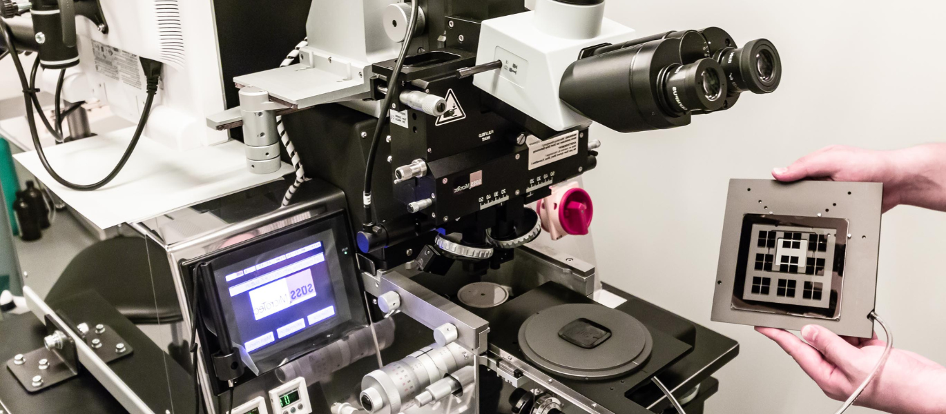
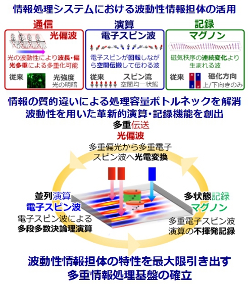
We are developing an information processing infrastructure that can utilize wave-like information carriers between communication, computation, and recording. These carriers will be based on optical waves, electron spin waves, and magnons which are waves generated by modulating magnetic order. This is based on hybrid structures comprising III-V semiconductor quantum structures and ferromagnetic materials, which exhibit excellent electrical conductivity and optical response.
The information infrastructure incorporating electron spin waves represents an as yet unexplored area of both academic research and device applications. Consequently, we would be interested in collaborating with researchers in order to advance our research.
Coming soon
Kohda Laboratory
Materials Science and Eng. Education and Reserch Buillding
Aoba-yama 02, Aoba-ku, Sendai 980-8579, JAPAN 980-8579
Phone : +81-22-795-7317
Copyright c 2023 Kohda Laboratory Tohoku University