Aims of This Project
The objective of this project is to promote research on the precise control of quantum states, structural analysis of novel quantum materials, and novel quantum properties with a view to integration with semiconductor and photonics technology. This integration will be achieved by highly controlling the spin states in semiconductor defects.
Moreover, we will concentrate on electron spin waves, which are novel information carriers based on the spatial structure of spins, and their quantum spin properties. Our objective is to develop new physical properties and establish novel functionalities for next-generation quantum information devices.
Project
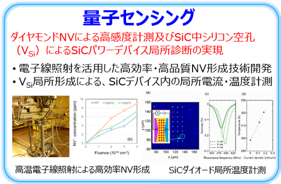
Local magnetic field measurement using diamond NV and SiC power device using silicon vacancy center in SiC (VSi)
(Quantum sensing research)
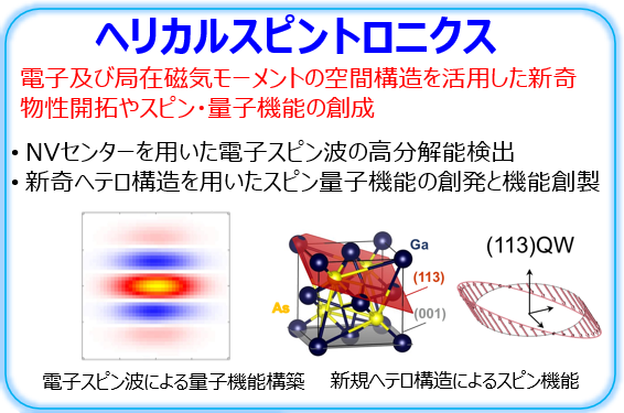
Development of novel physical properties and establishment of spin and quantum functionalities by utilizing the spatial structure of electrons and localized magnetic moments
(Helical Spintronics Research)
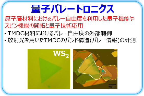
Exploitation of quantum and spin functionalities utilizing valley degrees of freedom in atomic layer materials and their application to quantum technology (Quantum Valletronics Research)
(Quantum valley electronics research)
Quantum Sensor Research Using Spin Defects in Wide-Gap Semiconductors
Quantum sensors represent a novel class of sensors that can measure various physical quantities, including magnetic field and temperature, with high sensitivity and high spatial resolution. This is achieved by exploiting the fact that electron spins of special defects, known as spin defects, formed in wide-gap semiconductors are highly sensitive to the surrounding environment.
Our research is focused on the exploration of new spin defects using two-dimensional materials, such as boron nitride, as well as three-dimensional materials, including diamond and silicon carbide, as parent materials. Additionally, we are engaged in research aimed at improving the performance of quantum sensors using existing or novel spin defects, with the objective of developing fundamental technology to support the future trillion-sensor era.
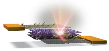
Helical Spintronics Research
By precisely controlling the effective magnetic field caused by spin-orbit interaction in semiconductor quantum structures, we exploit the persistent spin helix state that can both suppress spin relaxation and stabilize the spatial spin structure.
The objective is to establish techniques for the generation, control, and detection of electron spin waves that enable parallel and multiplexed information processing. This will facilitate the fusion of classical and quantum information technologies, which will take advantage of the multiplicity and parallelism of electron spin waves.
The objective is to elucidate magneto-transport and spatiotemporal spin dynamics in atomic layer materials and III-V semiconductor quantum structures for the electron spin wave properties. This will facilitate the development of fundamental technologies to support a future quantum society.
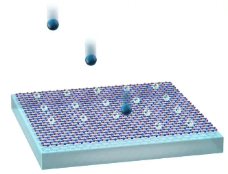
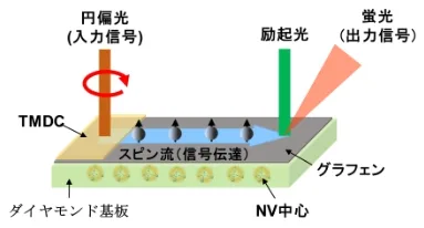
Atomic Layer Spin Sensing Research
The research will utilize spin defects in wide bandgap semiconductors that can detect spin information with high spatial resolution and high sensitivity. The objective is to conduct research on the spatial sensing of spin information in two-dimensional atomic layer materials, which have recently attracted attention as a stage for optical spin generation and spin current control.
The visualization of the spatial distribution of spin information is anticipated to be a novel technology for the advancement of a multitude of future spin-based devices, including ultra-low power consumption magnetic memory that will facilitate the emergence of a future quantum society.
The control of spin defects through the use of spin currents represents a promising avenue for future research.
Spin defect control utilizing spin currents
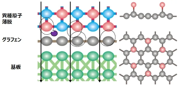
The Exploration of Novel Quantum Functional Materials
The objective of this research is the development of novel quantum functional materials that will facilitate the implementation of quantum technology in our society. The objective is to create new two-dimensional materials that can be utilized as wide bandgap semiconductors through the application of high-energy ion irradiation methods and surface science techniques.
The atomic structure and electronic state of these two-dimensional materials will be elucidated, and the generation of spin defects and stabilization of charge states will be controlled by controlling the atomic structure in order to realize quantum functionality.
Missionm01
Advanced Integration of Spin, Quantum, and Optical Technologies
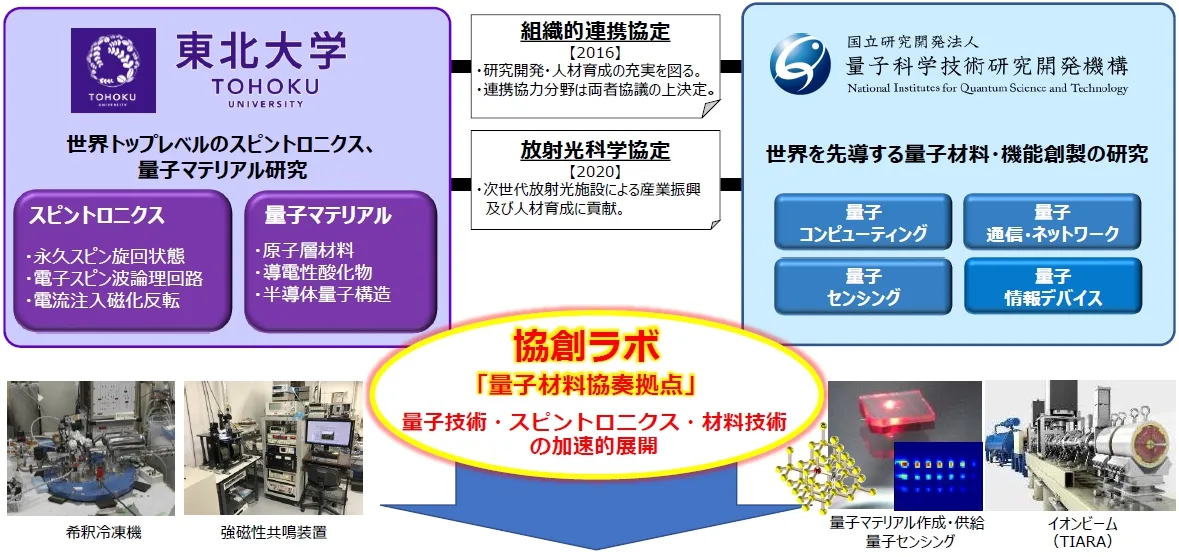
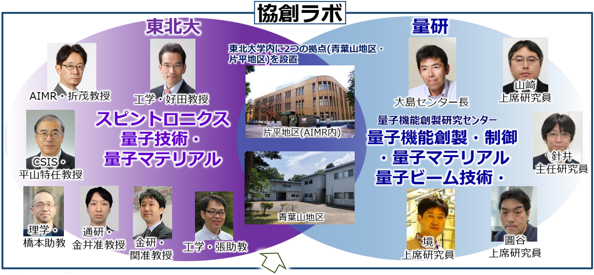
The establishment of a collaborative laboratory at Tohoku University that can highly integrate Tohoku University’s world-class research activities in spintronics and materials science with QST’s high-precision quantum beam technology for the creation of quantum materials and quantum functions will create a center for innovative research in quantum materials (CIRQuM). The CIRQuM is located in Tohoku University and the research results in CIRQuM transcend the boundaries of spintronics, materials science, and quantum technology. The collaborative laboratory in the CIRQuM will be located in the Katahira and Aobayama areas of Tohoku University, forming a hub where researchers from diverse fields can collaborate and accelerate joint research in the field of quantum technology.
Missionm02
Building a Quantum Society of the Future
In this joint research center, we will endeavor to maximize the research potential of the center for the innovative research in quantum materials “CIRQuM”, which will be a global center in quantum sensing and quantum functionalities, and Tohoku University, which boasts world-class expertise in spintronics and materials science. The collaboration will focus on spintronics and quantum materials research, with the objective of accelerating joint research and the development of quantum human resources. The aim is to accelerate the development of collaboration in quantum technology, spintronics, and materials science, with the ultimate goal of contributing to the construction of a quantum society of the future.

The objective of this research is to develop quantum materials science through collaboration between Tohoku University and the National Institute for Quantum Science and Technology.
In 2016, Tohoku University and the National Institute for Quantum Science and Technology (QST) concluded an organizational comprehensive collaboration agreement. In 2020, they entered into an agreement specialized in radiation science for the development and utilization of next-generation synchrotron radiation facilities. Since that time, they have been engaged in the promotion of next-generation synchrotron radiation research and the development of next-generation human resources. In FY2022, the “IIMR-Tohoku University Matching Research Support Program” (10 research projects) was initiated. In the field of quantum technology, where both institutes have strengths and where the national strategy “Vision for a Quantum Future Society” has been established, the two institutes will establish a collaborative laboratory based on their past collaboration to realize a quantum future society through the creation of quantum technology and quantum devices.
Realization of a Quantum Future Society through the Creation of Quantum Technology and Quantum Devices
The Tohoku University-QST : Center for Innovative Research for Quantum Materials (CIRQuM: Collaborative Laboratory)
Mission
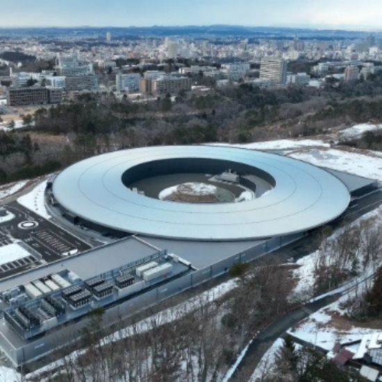
The establishment of a collaborative laboratory in Sendai (within Tohoku University), where the next-generation synchrotron radiation facility NanoTerasu is located, will facilitate the highly integrated Tohoku University research activities in spintronics and materials science with QST’s high-precision quantum beam technology for the creation of quantum materials and quantum functions. This will result in the creation of a center for research results that transcend the boundaries of spintronics, materials science (hydrogen science), and quantum technology.

Research Activities at the Tohoku University-QST Quantum Materials Collaboration Center